RF-BM-ND05 Bluetooth 5.0 pcb module nRF52840 Bluetooth Mesh for smart home
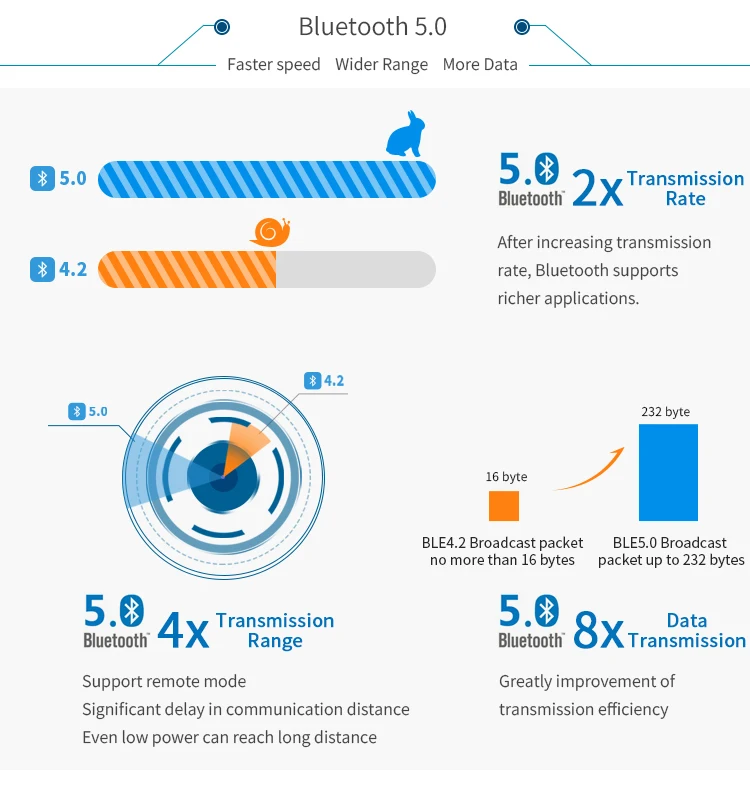
RF-BM-ND05 is an RF module based on Nordic Bluetooth 5.0 / / Thread / 802.15.4 / ANT / 2.4 GHz multiprotocol SoC -QIAA-R with best-in-class 32-bit ARM® Cortex®-M4 processor. It integrates a 32.768 kHz and a 32 MHz crystal, a power filter, an antenna matching, and a meander line inverted-F PCB antenna. It features high-performance digital interfaces, robust connection distance, and rigid reliability. It supports BLE stack v5.0 and can be preprogrammed with a serial interface communication protocol for simple programming. 1.27-mm pitch stamp stick package for easy assembling and cost-effective PCB design. RF-BM-ND05 is pin-to-pin compatible with .
Parameters of RF-BM-ND05
Chipset | nRF52840-QIAA-R |
Supply Power Voltage | 1.7 V ~ 5.5 V, recommended to 3.3 V |
Frequency | 2402 MHz ~ 2480 MHz |
Transmit Power | -20.0 dBm ~ +8.0 dBm (typical: 0 dBm) |
Receiving Sensitivity | -96 dBm |
GPIO | 29 |
Crystal | 32 MHz, 32.768 kHz |
RAM | 256 KB |
Flash | 1 MB |
Package | SMT Packaging |
Frequency Error | ±20 kHz |
Dimension | 24.8 mm x 15.0 mm x (2.3 ± 0.1) mm |
Type of Antenna | PCB antenna |
Operating Temperature | -40 ℃~ +85 ℃ |
Storage Temperature | -40 ℃~ +125 ℃ |


Recommended Footprint

Pin Attributes

Pin Functions of RF-BM-ND05
Pin | Name | Chip Pin | Pin Type | Description |
1 | GND | GND | GND | GND |
2 | VCC | VDD | Power | Power supply 1.7 V ~ 5.5 V, Recommend 3.3 V |
3 | P21 | P0_21 | I/O |
|
4 | P22 | P0_22 | I/O |
|
5 | P23 | P0_23 | I/O |
|
6 | P24 | P0_24 | I/O |
|
7 | P25 | P0_25 | I/O |
|
8 | P28 | P0_28 / AIN4 | I/O |
|
9 | P29 | P0_29/ AIN5 | I/O |
|
10 | P30 | P0_30 / AIN6 | I/O |
|
11 | P26 | P0_26 | I/O |
|
12 | P27 | P0_27 | I/O |
|
13 | P02 | P0_02 / AIN0 | I/O |
|
14 | P03 | P0_03 / AIN1 | I/O |
|
15 | P04 | P0_04 / AIN2 | I/O |
|
16 | P05 | P0_05 / AIN3 | I/O |
|
17 | P06 | P0_06 | I/O |
|
18 | P07 | P0_07 | I/O |
|
19 | P08 | P0_08 | I/O |
|
20 | P09 | P0_09 / NFC1 | I/O |
|
21 | P10 | P0_10 / NFC2 | I/O |
|
22 | P11 | P0_11 | I/O |
|
23 | P12 | P0_12 | I/O |
|
24 | P13 | P0_13 | I/O |
|
25 | P14 | P0_14 | I/O |
|
26 | P15 | P0_15 | I/O |
|
27 | P16 | P0_16 | I/O |
|
28 | SWDIO | SWDIO | I/O | Serial wire debug I/O for debug and programming |
29 | SWCLK | SWDCLK | I/O | Serial wire debug clock input for debug and programming |
30 | P17 | P0_017 | I/O |
|
31 | P18 / RST | P0_18 / RESET | I/O | Reset, active low. |
32 | P19 | P0_19 | I/O |
|
33 | P20 | P0_20 | I/O |
|


