TI CC3200 RF-WM-3200B3 Low Power Wi-Fi Module
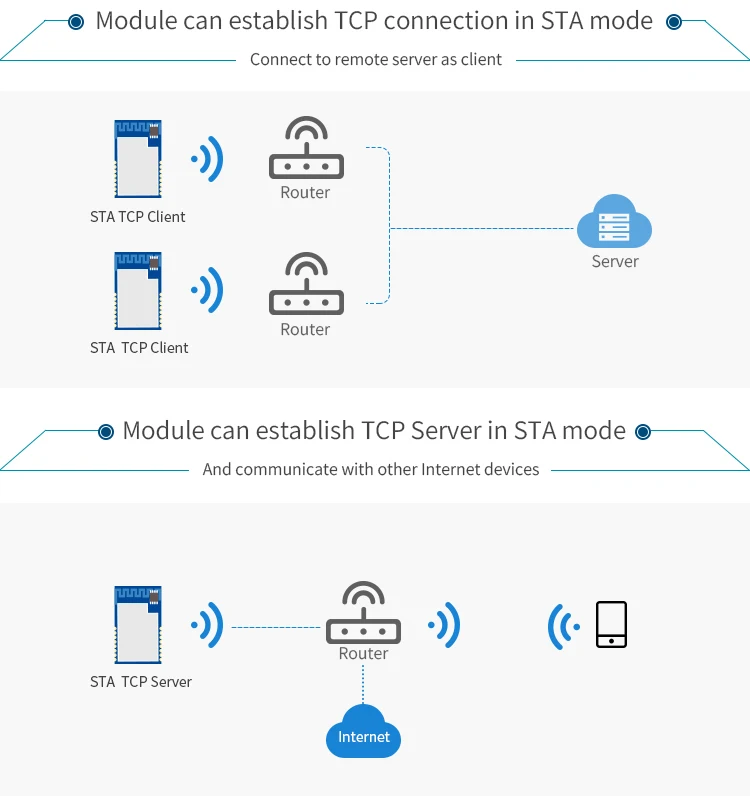
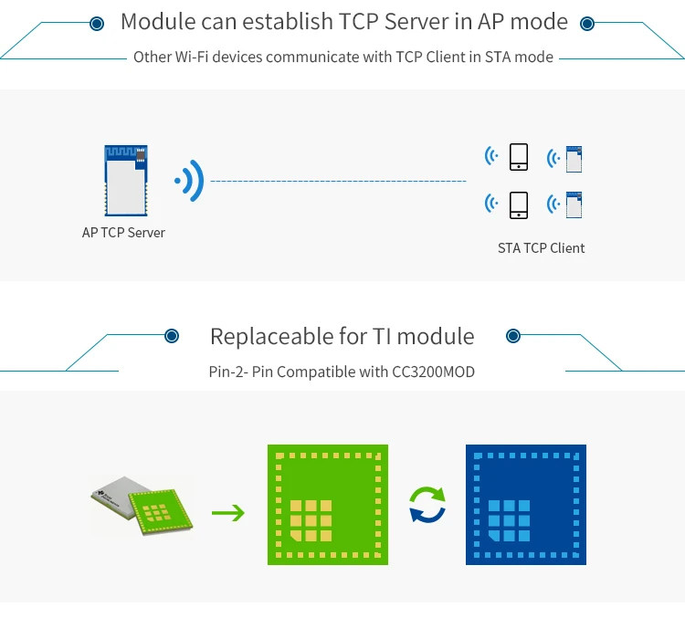
RF-WM-3200B3 Wi-Fi module is based on TI CortexTM-M4 core Wi-Fi SoC CC3200. It is of 63 pin, 17.50 mm x 20.50 mm, and 1.27 mm pitch LGA package, fully pin-to-pin compatible to TI CC3200MOD. This Wi-Fi module features the best-in-class low power consumption performance, integrates powerful crypto engine for fast and secured WLAN connections with 256-bit encryption, and supports WPA2 personal and enterprise security. This module complies with 2.4 GHz 802.11 b/g/n standards. Its TCP/IP stack that runs on chip supports up to 8 simultaneous TCP, UDP, or ROW sockets, or 2 simultaneous TLS v1.2 or SSL 3.0 sockets. It can run in Station, AP or Wi-Fi DirectTM connection modes. This module has integrated an SPI Flash, a sleep clock crystal, and a fast clock crystal. It supports a wide supply voltage range from 2.3 V to 3.6 V. It has a pin-out of peripherals of 8-bit parallel, I2S, SD/MMC, UART, SPI, I2C, ADC, DMA and GPIOs interfaces. It also comes with a preprogrammed data communication protocol over its serial port and an AT commands set to simplify customers’ operations on Wi-Fi configuration.
Parameters of RF-WM-3200B3
Chipset | CC3200 |
Supply Power Voltage | 2.3 V ~ 3.6 V, 3.3 V is recommended |
Frequency | 2.4 GHz |
Protocol | 802.11 b/g/n |
Transmit Power | +18.0 dBm @ 1 DSSS +14.5 dBm @ 54 OFDM |
Receiving Sensitivity | -95.7 dBm @ 1 DSSS -74.0 dBm @ 54 OFDM |
GPIO | 29 |
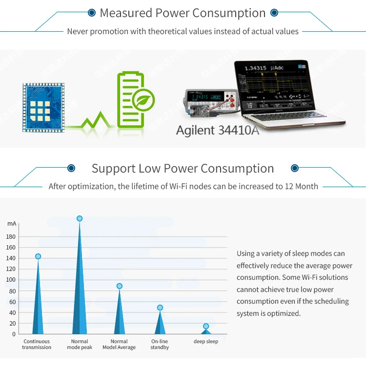
Power Consumption | Hibernate: 4 µA Low-power deep sleep (LPDS): 250 µA Idle connected (MCU in LPDS): 825 µA @ DTIM = 1 RX traffic (MCU active): 59 mA @ 54 OFDM TX traffic (MCU active): 229 mA @ 54 OFDM, maximum power |
Crystal | 40 MHz, 32.768 KHz |
Package | SMT packaging, half-hole packaging |
Communication Interface | UART, I2S, I2C, SPI, SD/MMC, ADC, DMA, PWM, McASP, Camera interface |
Dimension | 17.5 mm × 20.5 mm |
Operating Temperature | -40 ℃~ +85 ℃ |
Storage Temperature | -55℃~ +125 ℃ |


Recommended Footprint

Pin Attributes

Pin Functions of RF-WM-3200B3
Pin | Name | Chip Pin No. | Type | Function |
1 | GND |
| - | Ground |
2 | GND |
| - | Ground |
3 | GPIO10 | 1 | I/O | GPIO |
4 | GPIO11 | 2 | I/O | GPIO |
5 | GPIO14 | 5 | I/O | GPIO |
6 | GPIO15 | 6 | I/O | GPIO |
7 | GPIO16 | 7 | I/O | GPIO |
8 | GPIO17 | 8 | I/O | GPIO |
9 | GPIO12 | 3 | I/O | GPIO |
10 | GPIO13 | 4 | I/O | GPIO |
11 | GPIO22 | 15 | I/O | GPIO |
12 | JTAG_TDI / P23 | 16 | I/O | GPIO |
13 | NC | 13 | - | Reserved |
14 | NC | 14 | - | Reserved |
15 | NC | 11 | - | Reserved |
16 | GND |
| - | Ground |
17 | NC | 12 | - | Reserved |
18 | JTAG_TDO / P24 | 17 | I/O | GPIO |
19 | GPIO28 | 18 | I/O | GPIO |
20 | NC | 23 | - | Unused |
21 | JTAG_TCK / P19 | 19 | I/O | JTAG TCK input |
22 | JTAG_TMS / P29 | 20 | I/O | JTAG TMS input |
23 | SOP2 / P25 | 21 | I/O | Add pull-down resistor to ground needed for functional mode. Add option to pull-up required for entering the UART load mode for flashing. |
24 | SOP1 | 34 | - | Reserved. Do not connect. |
25 | ANTSEL1 / P26 | 29 | I/O | Antenna selection control. |
26 | ANTSEL2 / P27 | 30 | I/O | Antenna selection control. |
27 | GND |
| - | Ground |
28 | GND |
| - | Ground |
29 | NC | 27, 28 | - | Reserved |
30 | GND |
| - | Ground |
31 | RF_OUT1 | 31 | I/O | 2.4GHz RF input/output. |
32 | GND |
| - | Ground |
33 | NC | 38 | - | Reserved |
34 | SOP0 | 35 | - | Optional 1-kΩ pull-up if user chooses to use SWD debug mode instead of 4-wire JTAG. |
35 | RESET | 32 | I | Power on reset. Does not require external RC circuit. |
36 | VCC | 37 | - | Power supply for the device, can be connected to battery (2.7 V to 3.6 V). |
37 | VCC | 39 | - | Power supply for the device, can be connected to battery (2.7 V to 3.6 V). |
38 | GND |
| - | Ground |
39 | NC | 47 | - | Not connected |
40 | VCC | 10, 44, 54 | - | Power supply for the device, can be connected to battery (2.7 V to 3.6 V). |
41 | NC | 25, 36, 48 | - | Reserved |
42 | GPIO30 | 53 | I/O | GPIO |
43 | GND |
| - | Ground |
44 | GPIO0 | 50 | I/O | GPIO |
45 | NC | 51 | - | Reserved |
46 | GPIO1 | 55 | I/O | GPIO |
47 | GPIO2 | 57 | I/O | GPIO |
48 | GPIO3 | 58 | I/O | GPIO |
49 | GPIO4 | 59 | I/O | GPIO |
50 | GPIO5 | 60 | I/O | GPIO |
51 | GPIO6 | 61 | I/O | GPIO |
52 | GPIO7 | 62 | I/O | GPIO |
53 | GPIO8 | 63 | I/O | GPIO |
54 | GPIO9 | 64 | I/O | GPIO |
55 | GND |
| - | Thermal Ground |
56 | GND |
| - | Thermal Ground |
57 | GND |
| - | Thermal Ground |
58 | GND |
| - | Thermal Ground |
59 | GND |
| - | Thermal Ground |
60 | GND |
| - | Thermal Ground |
61 | GND |
| - | Thermal Ground |
62 | GND |
| - | Thermal Ground |
63 | GND |
| - | Thermal Ground |


